Search results
Search for "non-contact atomic force microscopy" in Full Text gives 34 result(s) in Beilstein Journal of Nanotechnology.
Studies of probe tip materials by atomic force microscopy: a review
Beilstein J. Nanotechnol. 2022, 13, 1256–1267, doi:10.3762/bjnano.13.104

- a homemade cantilevered non-contact atomic force microscopy (NC-AFM) system. As the first step of tip sharpening, the focus is on the controlled extraction of individual clusters. The experimental results show that controlled extraction of individual clusters induces a change in tip sharpness, which

Effects of focused electron beam irradiation parameters on direct nanostructure formation on Ag surfaces
Beilstein J. Nanotechnol. 2022, 13, 1004–1010, doi:10.3762/bjnano.13.87

- -contact atomic force microscopy (AFM) using the model Park NX10 AFM. The first experiment was conducted with beam current I as the variable parameter ranging from 7 to 500 pA. However, changing the value of I also changed the beam diameter d, which is a function of I and the working distance (WD). The
- changed while the other parameters were kept constant. The accelerating voltage U was equal to 30 kV in all experiments and the angle of incidence α was equal to 0°, unless stated otherwise. Following irradiation, the height and volume of the structures formed in irradiated points were determined by non


Two dynamic modes to streamline challenging atomic force microscopy measurements
Beilstein J. Nanotechnol. 2021, 12, 1226–1236, doi:10.3762/bjnano.12.90

- frequency is used as the set point. Historically, FM-AFM is commonly called non-contact atomic force microscopy [33]. However, repulsive forces are required to obtain high resolution, which implies some level of contact [34]. Qualitatively, this is easy to understand from the following reasoning. If a probe


Molecular assemblies on surfaces: towards physical and electronic decoupling of organic molecules
Beilstein J. Nanotechnol. 2021, 12, 950–956, doi:10.3762/bjnano.12.71

- . To a lesser extent, metal oxides have also been used, for which defects and charging often pose additional challenges [44][45][46]. On electronically insulating surfaces, non-contact atomic force microscopy (AFM) is the method of choice to study molecular assemblies and individual molecules in real
Local stiffness and work function variations of hexagonal boron nitride on Cu(111)
Beilstein J. Nanotechnol. 2021, 12, 559–565, doi:10.3762/bjnano.12.46

- non-contact atomic force microscopy (nc-AFM) to study h-BN on Cu(111). This template has interesting properties because the dielectric layer is only very weakly bound to the metal and shows an electronically induced Moiré superstructure [25][26]. First STM studies on this system pointed to only a


Determining amplitude and tilt of a lateral force microscopy sensor
Beilstein J. Nanotechnol. 2021, 12, 517–524, doi:10.3762/bjnano.12.42

- atomic force microscopy (AFM) is a non-contact atomic force microscopy technique where the frequency shift (Δf) of an oscillating tip is detected [1]. The frequency shift is a measure of the total force gradient acting on the tip, which includes both long-range and short-range contributions. A typical


Reconstruction of a 2D layer of KBr on Ir(111) and electromechanical alteration by graphene
Beilstein J. Nanotechnol. 2021, 12, 432–439, doi:10.3762/bjnano.12.35

- with unconventional stoichiometries have been observed indirectly on graphene surfaces [37]. Here, we report on the formation of irregularly shaped KBr islands with corrugated stripe structures, observed on the (111) surface of Ir and analyzed by non-contact atomic force microscopy (nc-AFM) at room


Protruding hydrogen atoms as markers for the molecular orientation of a metallocene
Beilstein J. Nanotechnol. 2020, 11, 1432–1438, doi:10.3762/bjnano.11.127

- acid (FDCA) molecules on bulk and thin film CaF2(111) surfaces with non-contact atomic force microscopy (NC-AFM). We use NC-AFM image calculations with the probe particle model to interpret this distinct shape by repulsive interactions between the NC-AFM tip and the top hydrogen atoms of the
- of the ferrocene moiety, herein on CaF2(111) surfaces, by using the protruding hydrogen atoms as markers. Keywords: calcium fluoride (CaF2); ferrocene; functionalised tips; high-resolution imaging; non-contact atomic force microscopy; Introduction It is still a challenge to determine the precise
- employed for the investigation of both ordered and unordered molecular systems as well as of individual and isolated species [4][5][6]. For example, two different non-planar isomers of dibenzo[a,h]thianthrene molecules could be identified by high-resolution non-contact atomic force microscopy (NC-AFM) [7


![[Graphic 10]](/bjnano/content/inline/2190-4286-11-127-i10.svg?max-width=637&scale=1.18182) row of FDCA molecules in geo 2. (a–c) Constant-height frequency-shi...
row of FDCA molecules in geo 2. (a–c) Constant-height frequency-shi...
Atomic defect classification of the H–Si(100) surface through multi-mode scanning probe microscopy
Beilstein J. Nanotechnol. 2020, 11, 1346–1360, doi:10.3762/bjnano.11.119

- Nanotechnology Research Centre, National Research Council Canada, Edmonton, Alberta, T6G 2M9, Canada 10.3762/bjnano.11.119 Abstract The combination of scanning tunnelling microscopy (STM) and non-contact atomic force microscopy (nc-AFM) allows enhanced extraction and correlation of properties not readily
- same side of two neighbouring dimers. Subsequently, the latter had been reassigned as an H, OH pair originating from dissociative attachment of a residual water molecule in the vacuum system [15][16][17]. Further insights became available by non-contact atomic force microscopy (nc-AFM), separating the


Measurement of electrostatic tip–sample interactions by time-domain Kelvin probe force microscopy
Beilstein J. Nanotechnol. 2020, 11, 911–921, doi:10.3762/bjnano.11.76

- Kalman filter; Kelvin probe force microscopy (KFM); time domain; Introduction Electrostatic forces are important interactions in non-contact atomic force microscopy (NC-AFM). They arise from differences in the work function of the tip and the sample, from trapped charges, or from potentials applied to


Atomic-resolution imaging of rutile TiO2(110)-(1 × 2) reconstructed surface by non-contact atomic force microscopy
Beilstein J. Nanotechnol. 2020, 11, 443–449, doi:10.3762/bjnano.11.35

- , because it cannot be clarified whether the (1 × 2) structure is formed over a wide area or only locally using macroscopic analysis methods such as diffraction. We used non-contact atomic force microscopy, scanning tunneling microscopy, and low-energy electron diffraction at room temperature to
- clean surface is relatively easy. A well-known rutile TiO2(110) surface is the (1 × 1) structure [2]. The (1 × 1) surface has been studied using low-energy electron diffraction (LEED) [3][4], surface X-ray diffraction [5], non-contact atomic force microscopy (NC-AFM) [6][7][8][9], scanning tunneling
- characterize the surface. Ti2O3 rows appeared as bright spots in both NC-AFM and STM images observed in the same area. High-resolution NC-AFM images revealed that the rutile TiO2(110)-(1 × 2) reconstructed surface is composed of two domains with different types of asymmetric rows. Keywords: non-contact atomic


Comparing a porphyrin- and a coumarin-based dye adsorbed on NiO(001)
Beilstein J. Nanotechnol. 2019, 10, 874–881, doi:10.3762/bjnano.10.88

- -layered islands on a NiO(001) single crystal surface have been studied by means of non-contact atomic force microscopy at room temperature. Comparison of both island types reveals different adsorption and packing of each dye, as well as an opposite charge-transfer direction, which has been quantified by
- Kelvin probe force microscopy measurements. Keywords: coumarin; Kelvin probe force microscopy; metal oxide; molecular resolution; nickel oxide (NiO); non-contact atomic force microscopy; porphyrin; Introduction With regard to its use in dye-sensitized solar cells (DSSCs), the wide-bandgap n-type
- -carboxyphenyl)porphyrin (Cu-TCPP) has been studied for the fabrication of n-type DSSCs [21][22]. In contrast, Coumarin 343 (C343) is an electron acceptor and is used for the design of p-type devices [23][24]. Both molecules structures are shown in Figure 1b. In this paper, non-contact atomic force microscopy


Review of time-resolved non-contact electrostatic force microscopy techniques with applications to ionic transport measurements
Beilstein J. Nanotechnol. 2019, 10, 617–633, doi:10.3762/bjnano.10.62

- atomic force microscopy. Here, we review in detail several time-resolved EFM techniques based on non-contact atomic force microscopy, elaborating on their specific limitations and challenges. We also introduce a new experimental technique that can resolve time-varying signals well below the oscillation


Combined pulsed laser deposition and non-contact atomic force microscopy system for studies of insulator metal oxide thin films
Beilstein J. Nanotechnol. 2018, 9, 686–692, doi:10.3762/bjnano.9.63

- a combined system of pulsed laser deposition (PLD) and non-contact atomic force microscopy (NC-AFM) for observations of insulator metal oxide surfaces. With this system, the long-period iterations of sputtering and annealing used in conventional methods for preparing a metal oxide film surface are
- transmission electron microscopy [5][8][9][10][11][12][13]. As atomic resolution methods, scanning probe microscopy including scanning tunneling microscopy (STM) [13][14][15][16][17][18][19][20][21][22][23][24][25][26][27][28][29][30] and non-contact atomic force microscopy (NC-AFM) [19][23][29][31][32][33][34


Anchoring of a dye precursor on NiO(001) studied by non-contact atomic force microscopy
Beilstein J. Nanotechnol. 2018, 9, 242–249, doi:10.3762/bjnano.9.26

- non-contact atomic force microscopy at room temperature. Depending on the coverage, single molecules, groups of adsorbates with random or recognizable shapes, or islands of closely packed molecules were identified. Single molecules and self assemblies are resolved with submolecular resolution showing
- (II) oxide (NiO); non-contact atomic force microscopy; p-type semiconductor; sub-molecular resolution; Introduction Inorganic substrates functionalized with organic molecules are nowadays highly regarded materials for emerging hybrid technologies including molecular electronics, photocatalysts or
- lie between 3.5 and 4.3 eV [25][26][27][28][29], and given that scanning tunnelling microscopy (STM) can only be performed on thin NiO films grown on metals [30][31], non-contact atomic force microscopy (nc-AFM) in ultra-high vacuum is the technique of choice. Due to its hardness and high reactivity


Optimizing qPlus sensor assemblies for simultaneous scanning tunneling and noncontact atomic force microscopy operation based on finite element method analysis
Beilstein J. Nanotechnol. 2017, 8, 657–666, doi:10.3762/bjnano.8.70

- ; noncontact atomic force microscopy; quartz tuning forks; scanning tunneling microscopy; self-sensing probe; Introduction Scanning tunneling microscopy (STM) [1] and non-contact atomic force microscopy (NC-AFM) [1][2][3] are powerful methods allowing the visualization of the atomic structure of a surface


Noise in NC-AFM measurements with significant tip–sample interaction
Beilstein J. Nanotechnol. 2016, 7, 1885–1904, doi:10.3762/bjnano.7.181
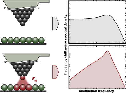
- & Astronomy, The University of Nottingham, University Park, Nottingham NG7 2RD, UK 10.3762/bjnano.7.181 Abstract The frequency shift noise in non-contact atomic force microscopy (NC-AFM) imaging and spectroscopy consists of thermal noise and detection system noise with an additional contribution from
- : amplitude noise; cantilever stiffness; closed loop; detection system noise; frequency shift noise; non-contact atomic force microscopy (NC-AFM); Q-factor; spectral analysis; thermal noise; tip–sample interaction; Introduction Non-contact atomic force microscopy (NC-AFM) [1][2] is an unmatched surface


![[Graphic 32]](/bjnano/content/inline/2190-4286-7-181-i73.png?max-width=637&scale=1.18182) wit...
wit...

![[Graphic 34]](/bjnano/content/inline/2190-4286-7-181-i75.png?max-width=637&scale=1.18182) wit...
wit...


Scanning probe microscopy studies on the adsorption of selected molecular dyes on titania
Beilstein J. Nanotechnol. 2016, 7, 1642–1653, doi:10.3762/bjnano.7.156

- ). Jöhr et al. used non-contact atomic force microscopy and KPMF to study the adsorption and interaction of copper(II) meso-tetra(4-carboxyphenyl)porphyrin (Cu-TCPP) on a TiO2(110) surface in a submonolayer coverage regime at room temperature [60]. First, the authors identified two dominant adsorption


Noncontact atomic force microscopy III
Beilstein J. Nanotechnol. 2016, 7, 946–947, doi:10.3762/bjnano.7.86
- every year at the annual “International Conference on Non-Contact Atomic Force Microscopy” series, which is typically characterized by lively discussions on the latest technical and scientific developments related to NC-AFM. In parallel with the series of conferences, the last few years have seen the
Modelling of ‘sub-atomic’ contrast resulting from back-bonding on Si(111)-7×7
Beilstein J. Nanotechnol. 2016, 7, 937–945, doi:10.3762/bjnano.7.85

- force mapping of atomic and molecular structures using non-contact atomic force microscopy (NC-AFM). In particular, suppressing the chemical bonding between tip and sample enables the stable exploration of the repulsive part of the tip–sample force regime, which has allowed outstanding resolution to be


Virtual reality visual feedback for hand-controlled scanning probe microscopy manipulation of single molecules
Beilstein J. Nanotechnol. 2015, 6, 2148–2153, doi:10.3762/bjnano.6.220

- advantages of the set-up are demonstrated by applying it to the model problem of the extraction of an individual PTCDA molecule from its hydrogen-bonded monolayer grown on Ag(111) surface. Keywords: non-contact atomic force microscopy (NC-AFM); Oculus Rift; perylene-3,4,9,10-tetracarboxylic dianhydride


A simple method for the determination of qPlus sensor spring constants
Beilstein J. Nanotechnol. 2015, 6, 1733–1742, doi:10.3762/bjnano.6.177

- ; calibration; non-contact atomic force microscopy; qPlus; Introduction Non-contact-atomic force microscopy (ncAFM) has paved new inroads to the measurement of nanometer-scale properties that were previously inaccessible. By allowing the atomic-scale imaging of surfaces from insulators to conductors, the


![[Graphic 9]](/bjnano/content/inline/2190-4286-6-177-i28.png?max-width=637&scale=1.18182) vs b is plotted where kI is the spring constan...
vs b is plotted where kI is the spring constan...
Lower nanometer-scale size limit for the deformation of a metallic glass by shear transformations revealed by quantitative AFM indentation
Beilstein J. Nanotechnol. 2015, 6, 1721–1732, doi:10.3762/bjnano.6.176

- Abstract We combine non-contact atomic force microscopy (AFM) imaging and AFM indentation in ultra-high vacuum to quantitatively and reproducibly determine the hardness and deformation mechanisms of Pt(111) and a Pt57.5Cu14.7Ni5.3P22.5 metallic glass with unprecedented spatial resolution. Our results on


Nano-contact microscopy of supracrystals
Beilstein J. Nanotechnol. 2015, 6, 1229–1236, doi:10.3762/bjnano.6.126

- tunnelling microscopy and spectroscopy. Keywords: dynamic force microscopy; nanoparticle; non-contact atomic force microscopy; point contact imaging; scanning probe microscopy; supracrystal; Introduction Artificial solids comprising extended assemblies of nanocrystals with a narrow size distribution

![[Graphic 1]](/bjnano/content/inline/2190-4286-6-126-i1.png?max-width=637&scale=1.18182) = 20 pA, ...
= 20 pA, ...


Magnetic properties of self-organized Co dimer nanolines on Si/Ag(110)
Beilstein J. Nanotechnol. 2015, 6, 777–784, doi:10.3762/bjnano.6.80

- ]. We note that these protrusions are too large to represent individual atoms. We have recently shown that neither STM nor non-contact atomic force microscopy (nc-AFM) probes can straightforwardly resolve the inner atomic structure of the Si NRs [25]. All NRs, varying only in length, present the same


